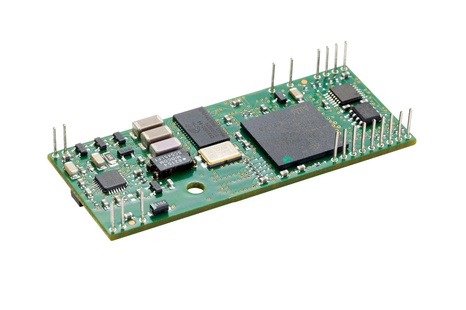
Found in everyday devices such as smartphones, computers, TVs, and home appliances, Printed Circuit Board Assemblies or PCBAs play a pivotal role in electronic manufacturing. Electrical components are mounted onto the PCB using a variety of techniques.
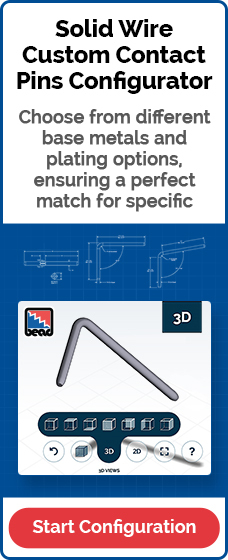
Bead Electronics has extensive experience working with PCB design and electrical engineers to manufacture pins that will leverage pin insertion technology to work seamlessly with your PCB or loose pins to support a custom connector design.
Download our free Plated Through Hole Size Guide
When it comes to PCB design, you may want to use through-hole, surface mount or press-fit mounting techniques, depending on the needs of your product.
Here are some tips to decide which mounting technique is right for your project.
What is Through-Hole Technology?
One of the oldest PCB mounting techniques around, through-hole technology (THT) involves drilling holes into the PCB and inserting leads into the through-hole component and soldering the leads into pads on the opposite side of the PCB. Depending on the scale of production, the lead insertion and soldering can either be done manually or with automation. As a result, these components take up board real estate on both sides of the PCB.
Some components that are commonly mounted with this technique include resistors, capacitors and inductors. While these components are more common, some connectors or other larger devices also leverage THT. Through-hole components tend to be on the larger side, as opposed to surface mounting. Because of this, the components will take up more space on the PCB, however; larger components come in handy when you need to make manual adjustments.
Benefits of Through-Hole Technology
Using through-hole technology to mount components creates a strong mechanical bond, particularly useful in automotive, aerospace or military applications where the components may be subjected to physical stress. Components mounted using through-hole technology are also more heat tolerant than their surface-mounted counterparts, making them ideal for industrial applications.
In addition, THT can be used for low-volume or prototype applications. Components made with THT can be easier to solder by hand and don’t require tooling or silkscreens.
Limitations of Through-Hole Technology
The larger components required for through-hole mounting means less PCB space. In addition, you cannot use the backside of the PCB in the hole location as well. The space constraint impacts the number of components that can be added, the routing of signal trees and the overall performance of the circuit. As electronic devices get smaller and smaller, the demand for smaller PCBs is on the rise.
Because of the multiple steps involved in this mounting technique, production may be more time-consuming, expensive and produces more waste.
The longer leads required for through-hole mounting can cause distortion at high frequencies, making through-hole mounting less suited for telecommunications applications.
When to Use Through-Hole Technology
A robust and highly reliable option, you should consider using through-hole technology for:
- Parts that will be subjected to physical stress or harsh conditions
- Prototyping stages where manual adjustments may be needed
- Small-scale production
What is Surface Mount Technology?
A more modern approach to PCB mounting, surface mount technology is when components are soldered directly to pads on the PCB. The soldering is typically done through automation, although for small-scale production, it can be done manually.
When using surface mounting techniques, components can be mounted on both sides of the PCB and the components can be much smaller in size.

Benefits of Surface Mount Technology
With smaller components, PCBs made with surface mount technology can have more complex circuitry while still being compact, making them ideal for handheld electronics. Because this mounting technique can be fully automated, production is faster, removes the possibility of human error and creates less waste than through-hole technology.
The shorter leads in surface-mounted components mean less distortion at high frequency, making this method ideal for telecommunications applications.
Limitations of Surface Mount Technology
The smaller size of surface-mounted components makes them more fragile and susceptible to damage, especially in harsh conditions. PCBs manufactured using this method are also more difficult to modify because of the small components.
Although surface mounting is more cost-effective and efficient than through-hole technology in the long run, the initial investment in developing stencils and purchasing automated equipment is significant.
If you need the strength of a through-hole pin but want to use SMT for production, check out our solutions for True Grip Pins here.
When to Use Surface Mount Technology
Known for making more compact and efficient PCBs, surface mount technology is a good option for:
- Large-scale production
- Handheld or smaller electronics
- High-frequency applications
What is Press-Fit Technology?
Unlike the other two processes, press-fit technology mounts components to the PCB without soldering. Instead, a press-fit pin, connector or device is inserted into the through-hole plating of the PCB and secured using cold welding. There are two types of press-pins: solid and elastic. Solid pins have low tolerance but more stability, while elastic pins, also known as compliant pins, have higher tolerance and are more compliant. The pins can either be installed manually or with automation.
Benefits of Press-Fit Technology
Without soldering, the production process is faster, more environmentally friendly and avoids putting thermal stress on the components. The result is a PCB with highly reliable components and a lower failure rate than those with solder joints. Removing soldering from the process also makes it easier to repair or place components if needed. Using an automated press-fit process means long-term cost savings.
Without soldering, compliant press-fit connectors have better signal integrity, suitable for high speed/frequency applications; however, as you increase signal speed, you also increase the cost of your components.
With this method, components can be applied to one or both sides of PCBs in a wide range of thicknesses.
Limitations of Press-Fit Technology
Each type of press-pin has some limitations. Solid pins have a greater chance of damaging the PCB during installation, have greater sensitivity to shock and vibration, and have shorter life cycles. Elastic or compliant pins are less likely to cause damage during installation and have longer life cycles.
Selecting the right materials for the pins is crucial to their performance. For example, gold-plated pins should not be combined with a chemical gold surface. To ensure the mounting process works correctly, either the PCB surface or the pin should be tinned. If there isn’t enough friction between the pin and the PCB, the bond won’t last or be able to withstand pressure.
Although this method is cost-effective in the long run, the initial investment in equipment is significant. Additionally, for large-scale production, using pins may not be the most efficient.
When to Use Press-Fit Technology
A revolutionary solderless mounting technique, press-fit technology should be considered for:
- Power applications that need high conductivity
- Small devices that require complex circuitry
- Unique productions
PCB Solutions at Bead Electronics
Choosing between through-hole, surface and press-fit mounting techniques will depend on the specific needs of your product. For components that will be subjected to physical stress, high temperatures or other harsh conditions, the strong mechanical bond provided by through-hole technology is unmatched. When it comes to making compact devices with complex circuitry, you’ll want to consider surface or press-fit mounting.
Bead Electronics has a long history of providing pins for a variety of Printed Circuit Board applications in industries such as automotive, telecom, aerospace, industrial, medical and more.
Bead's contact pins can be used for power, signal, or even electro-mechanical applications as part of printed circuit boards.
For a quick reference on pin sizes, tolerances, and feature types, download this free helpful one-page resource.